

Parametry
Więcej o książce
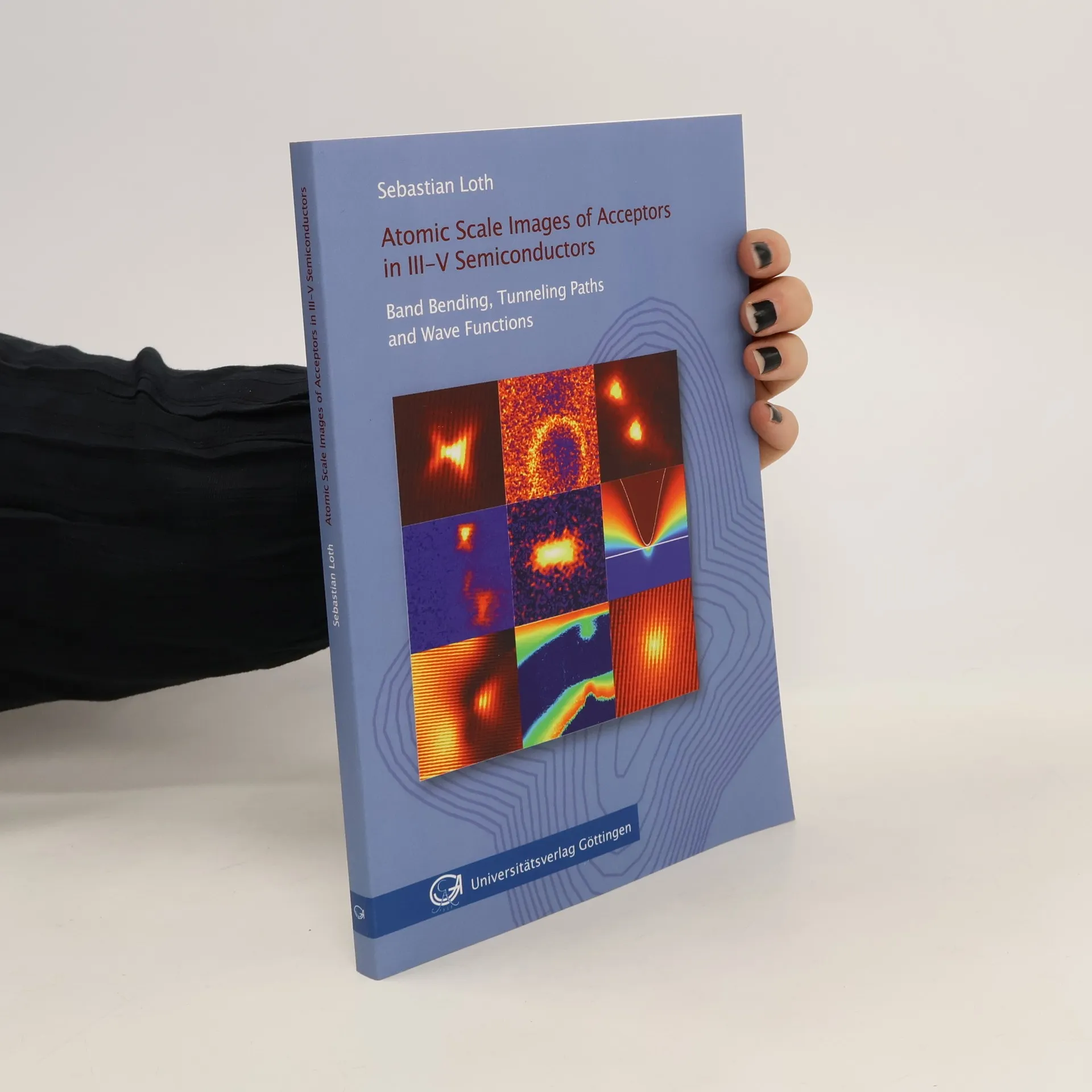
This volume reports measurements of single dopant atoms in III-V semiconductors with low temperature scanning tunneling microscopy (STM) and scanning tunneling spectroscopy (STS). It studies the anisotropic spatial distribution of acceptor induced tunneling processes at the {110} cleavage planes. Two different tunneling processes are identified: conventional imaging of the squared acceptor wave function and resonant tunneling at the charged acceptor. A thorough analysis of the tip induced space charge layers identifies characteristic bias windows for each tunnel process. The symmetry of the host crystal's band structure determines the spatial distribution of the tunneling paths for both processes. Symmetry reducing effects at the surface are responsible for a pronounced asymmetry of the acceptor contrasts along the principal [001] axis. Uniaxial strain fields due to surface relaxation and spin orbit interaction of the tip induced electric field are discussed on the basis of band structure calculations. High-resolution STS studies of acceptor atoms in an operating p-i-n diode confirm that an electric field indeed changes the acceptor contrasts. In conclusion, the anisotropic contrasts of acceptors are created by the host crystal's band structure and concomitant symmetry reduction effects at the surface.
Zakup książki
Atomic scale images of acceptors in III-V semiconductors, Sebastian Loth
- Język

- Rok wydania
- 2008
- Oprawa
- (miękka)
Metody płatności
Nikt jeszcze nie ocenił.
- Tytuł
- Atomic scale images of acceptors in III-V semiconductors
- Język
- angielski
- Autorzy
- Sebastian Loth
- Wydawca
- Univ.-Verl. Göttingen
- Rok wydania
- 2008
- Oprawa
- miękka
- ISBN10
- 3940344141
- ISBN13
- 9783940344144
- Seria
- Kategorie
- Opis
- This volume reports measurements of single dopant atoms in III-V semiconductors with low temperature scanning tunneling microscopy (STM) and scanning tunneling spectroscopy (STS). It studies the anisotropic spatial distribution of acceptor induced tunneling processes at the {110} cleavage planes. Two different tunneling processes are identified: conventional imaging of the squared acceptor wave function and resonant tunneling at the charged acceptor. A thorough analysis of the tip induced space charge layers identifies characteristic bias windows for each tunnel process. The symmetry of the host crystal's band structure determines the spatial distribution of the tunneling paths for both processes. Symmetry reducing effects at the surface are responsible for a pronounced asymmetry of the acceptor contrasts along the principal [001] axis. Uniaxial strain fields due to surface relaxation and spin orbit interaction of the tip induced electric field are discussed on the basis of band structure calculations. High-resolution STS studies of acceptor atoms in an operating p-i-n diode confirm that an electric field indeed changes the acceptor contrasts. In conclusion, the anisotropic contrasts of acceptors are created by the host crystal's band structure and concomitant symmetry reduction effects at the surface.