

Więcej o książce
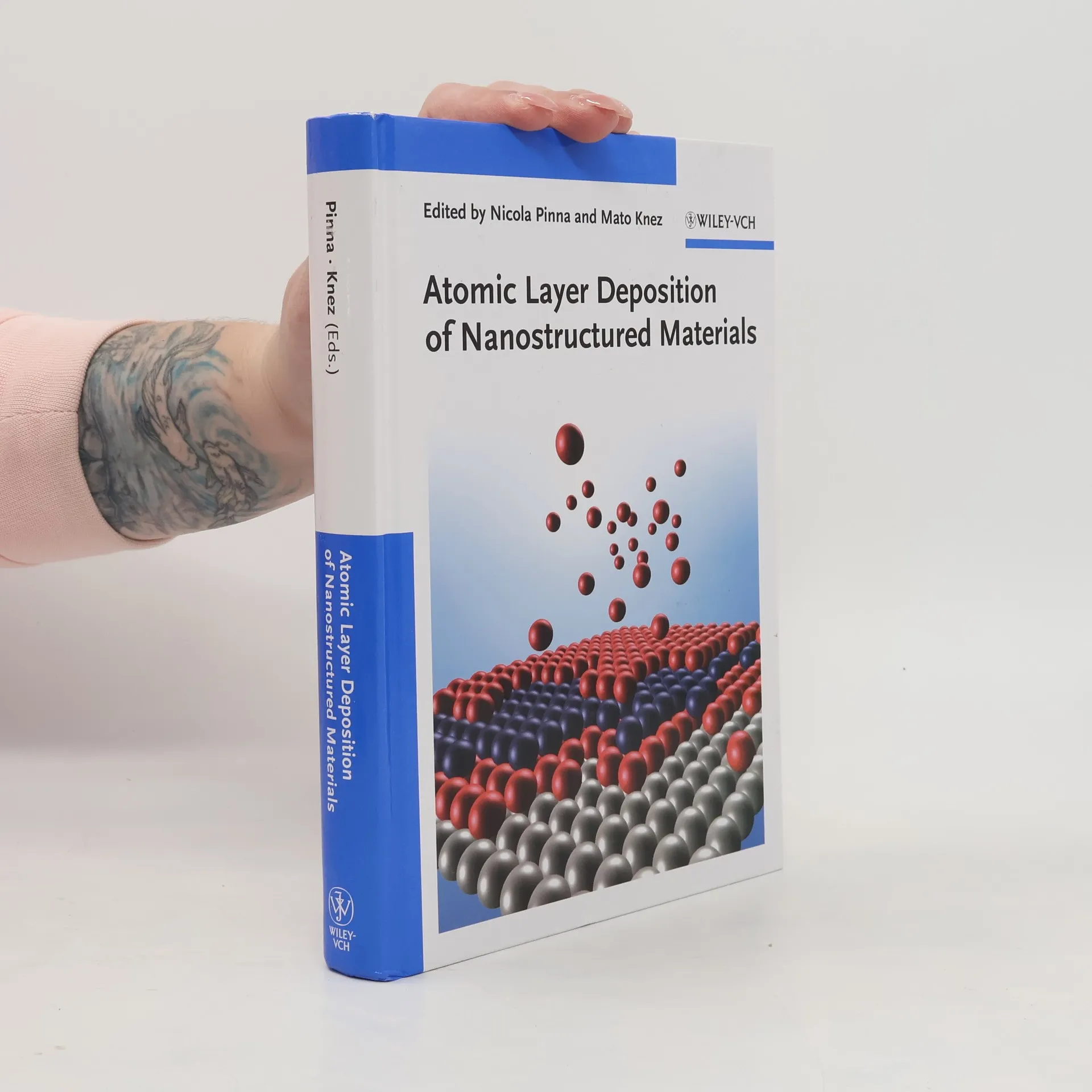
Atomic layer deposition, formerly called atomic layer epitaxy, was developed in the 1970s to meet the needs of producing high-quality, large-area fl at displays with perfect structure and process controllability. Nowadays, creating nanomaterials and producing nanostructures with structural perfection is an important goal for many applications in nanotechnology. As ALD is one of the important techniques which offers good control over the surface structures created, it is more and more in the focus of scientists. The book is structured in such a way to fi t both the need of the expert reader (due to the systematic presentation of the results at the forefront of the technique and their applications) and the ones of students and newcomers to the fi eld (through the first part detailing the basic aspects of the technique).This book is a must-have for all Materials Scientists, Surface Chemists, Physicists, and Scientists in the Semiconductor Industry.
Zakup książki
Atomic Layer Deposition of Nanostructured Materials, Nicola Pinna, Mato Knez
- Język

- Rok wydania
- 2011
- Oprawa
- (twarda)
Metody płatności
Nikt jeszcze nie ocenił.
- Tytuł
- Atomic Layer Deposition of Nanostructured Materials
- Język
- angielski
- Autorzy
- Nicola Pinna, Mato Knez
- Wydawca
- Wiley-VCH
- Rok wydania
- 2011
- Oprawa
- twarda
- Liczba stron
- 472
- ISBN10
- 3527327975
- ISBN13
- 9783527327973
- Seria
- Opis
- Atomic layer deposition, formerly called atomic layer epitaxy, was developed in the 1970s to meet the needs of producing high-quality, large-area fl at displays with perfect structure and process controllability. Nowadays, creating nanomaterials and producing nanostructures with structural perfection is an important goal for many applications in nanotechnology. As ALD is one of the important techniques which offers good control over the surface structures created, it is more and more in the focus of scientists. The book is structured in such a way to fi t both the need of the expert reader (due to the systematic presentation of the results at the forefront of the technique and their applications) and the ones of students and newcomers to the fi eld (through the first part detailing the basic aspects of the technique).This book is a must-have for all Materials Scientists, Surface Chemists, Physicists, and Scientists in the Semiconductor Industry.